


Spectroscopy Investigation of Nanostructures Utilizing the Park AFM Instruments
Case Study: Zinc Oxide Nanostructures
BY T.A. Merz, D.R. Doutt, and L.J. Brillson
Department of Physics, Ohio State University
General Considerations
Zinc Oxide (ZnO) is increasingly gaining attention in the research community because of its excellent bulk properties -- high exciton binding energy, high sensitivity to adsorbate charge transfer, and high carrier mobility -- but also, more recently, because of its remarkable ability to grow nanostructures. There has been much research done in the development of growth procedures and increasing the understanding of the growth mechanisms for induced nanostructures and their use in devices[i],[ii]. However, there has been very little work done on the examination of electronic properties on the nanoscale and how these properties feed into the nucleation and growth of said nanostructures or how these electronic properties affect the ability to make reliable Schottky contacts to ZnO[iii]. Furthermore, the exploration of nanostructures has yet to venture into the realm of spontaneous structure growth.
The ability to understand and thus potentially control how electronic, morphological, and chemical disparities all play a synergistic role in the behavior of ZnO devices should be a high priority of all those currently investigating ZnO as an electronic material and especially those that are looking to use it to make nanoscale devices. The investigation of this trinity of defects -- electronic, morphological, and chemical -- on the nanoscale is by no means an easy task and might explain the relative lack of work on the topic. There are a number of techniques that are capable of looking at one or two of these properties on a localized scale, most notably SEM with depth resolved cathodoluminescence or AFM/KPFM, but being able to examine all three simultaneously at a reasonable price has evaded many well meaning attempts.
Figure 1 shows one sample of these spontaneous nanostructures formed on a Zn-polar ZnO surface as imaged by a Park AFM. The alignment of these nanostructures along crystallographic directions is shown in Fig. 1 as well as a close up of a string of nano-mounds highlighting the trenches surrounding the base of each mound, shown as a break out on the right side. This map emphasizes the complexity and compound nature of the spontaneous nanostructure growth that is spontaneously possible.
It is through the scanning probe revolution that we are able to offer a cluster of three techniques that allow one to probe the electronic, morphological, and chemical landscape of any semiconducting sample in ambient conditions. The use of AFM and KPFM allow for the simultaneous mapping of the morphological and electronic features of a sample while the inclusion of nanoscale surface photovoltage spectroscopy (SPS) allows for the probing of chemical defects at isolated positions, which can be selected from either AFM or KPFM maps, or over large regions.
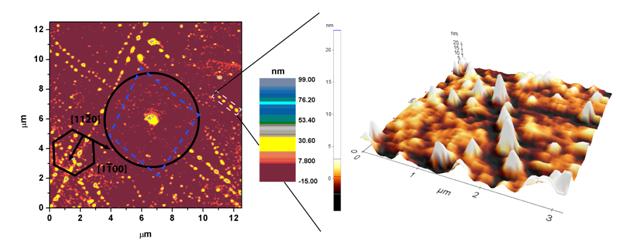
Figure 1. Spontaneous nanostructure growth on the Zn-polar surface of ZnO.
Park AFM System and Nanoscale Surface Photovoltage Spectroscopy Overview
At the core of the nanoscale SPS is the Park AFM/KPFM with the Enhanced EFM module. The Park's unique open head design allows for an optical fiber to be brought into close proximity to the sample's surface. This geometry permits us to illuminate the sample surface with monochromatic light while the AFM/KPFM mode is enabled and scanning. With increasing photon energy above characteristic threshold values, the light pumps carriers into and out of surface states within the semiconductor bandgap, changing the band bending and the Fermi level at the surface, which can be simultaneously monitored with the KPFM module. Changes that are seen in the KPFM signal may then be interpreted as movement of the Fermi level because of the population/depopulation of such surface or defect states through optical excitation. The energy of photons at which the KPFM signal changes offers the relative energy of the transition and therefore the characteristic energy of the defect level and the sign of the change in KPFM signal pins down whether the characteristic energy is relative to the valence band or the conduction band. This allows for the exact determination of defect states within the bandgap on a localized scale: a marked improvement over traditional luminescence techniques where only energy differences are possible to determine. Figure 2 shows the schematic setup of a nanoscale SPS setup. The metalized cantilever, PSPS, and laser diode are all contained within the Park AFM/KPFM system.
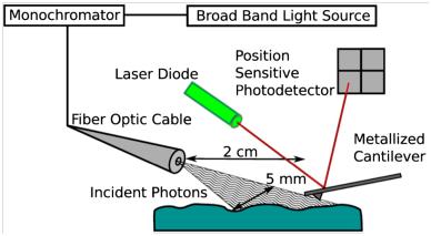
Figure 2. Schematic of the nanoscale SPS monochromatized light source positioned near a Park Systems KPFM cantilever. The tip of the fiber optic cable is 2 cm from the metalized tip and illuminates a 5 mm diameter spot.
Investigation of ZnO Nanostructures
Figure 3 shows two simultaneous maps (a) and (b) acquired with a Park AFM and Enhanced EFM mode respectively. The two maps are from the Zn-polar surface of an air exposed ZnO single crystal. Three separate regions, of two distinct types, are visible in the maps. The three regions are labeled with markers (1), (2), and (3). Regions (1) and (3) show a high concentration of nano-mounds as evident in the AFM map; the regions also show a markedly lower EFM signal than region (2) which is relatively smooth topographically. Figures 3(c), (d), and (e) show corresponding SPS spectra from the localized points (1), (2), and (3). For the regions with nanostrcuture growth there is an obvious extra feature in the SPS spectra beside the bandgap response at 3.34 eV, that is absent in the smooth region's SPS spectra. The feature in Fig. 3 (c) and (e) are from a surface defect at 1.7-1.8 eV below the conduction band, which is connected by other experimental evidence to the VZn[iv]. The use of all three of these techniques together allows a complete picture of the topographical, electronic, and chemical structure on the nanoscale.
Figure 4 (a) shows an AFM map highlighting the area near one isolated nano-mound from another Zn-polar. Four SPS spectra were taken from four separate places on the AFM map, each of the four places farther from the tip of the nano-mound than the last. Figure 4 (b), (c), (d), and (e) show the SPS spectra from these four points which correspond to positions at the peak of the nano-mound (b), at the edge of the nano-mound (c), 350 nm from the edge of the nano-mound, and 750 nm from the edge of the nano-mound. At each of these locations there is an obvious change in the defect level at 2.1 eV, demonstrating a resolution for chemical analysis of better than 100 nm. A more complete analysis and demonstration of the nanoscale SPS is written up elsewhere[v].
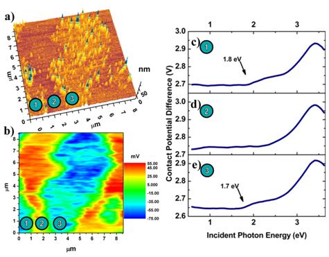
Figure 3. (a) AFM map of ZnO(000 ī) surface with two adjoining surface morphologies: a 1.27 nm rms smooth surface region (2) bounded by surfaces with clustered nano-mounds (1 and 3). (b) KPFM map from the same area. Regions (1) and (3) show lower CPD (larger Φ) than (2). SPS spectra (c) and (e), respectively show clear onsets at 1.7–1.8 eV that are absent in spectrum (2).
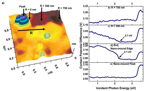
Figure 4. (a) Topographical map of a single nano-mound on a ZnO(0001) face. Spectra show: (b) no evidence of a 2.1 eV feature, (c) a positive CPD change at 2.1 eV, (d) a larger CPD slope change at 2.1 eV at the nano-mound edge, and (e) no evidence of gap states atop nano-mound.
Conclusion
The ability to simultaneously image topographical, chemical, and electronic local environments on the nanometer scale is not only a highly powerful technique for understanding the basic physics of materials, but it is also is very useful in examining device structures and their failure mechanisms[vi]. Through the ability to examine and interpret material behavior in a complete way, non-destructive way it may become possible to then control material behavior with these insights. The combination of AFM/KPFM/SPS offers the perfect complement of techniques to measure these three different, but related, local environments. The Park AFM/KPFM has proven to be superior to other designs by having an open design where additions and complementary equipment may be included by the end user to flexibly change their system to do the unique tasks that they wish to accomplish which in turn further both scanning probe technology and basic science.
Note
This work was supported by the National Science Foundation under Award No. DMR-0803276 (Verne Hess and Charles Ying) under a Research Experience for Undergraduates.
References
[i] S.J. Pearton, D.P. Norton, D.P., K. Ip, Y.W. Heo, T. Steiner, Prog.Mater. Sci. 50 (2005) 293.
[ii] L. Schmidt-Mende, J.L. MacManus-Driscoll, Mater. Today 10 (2007) 40.
[iii] L.J. Brillson, H.L. Mosbacker, M.J. Hetzer, Y. Strzhemechny, G.H. Jessen, D.C. Look. G. Cantwell, J. Zhang, and J.J. Song, Appl. Phys. Lett. 90 (2007) 102116.
[iv] Y. Dong, F. Tuomisto, B.G. Svensson, A.Y. Kuznetsov and L.J. Brillson, Phys. Rev. B. 81 (2010) 081201.
[v] T.A. Merz, D.R. Doutt, T. Bolton, Y. Dong, and L.J. Brillson, Surf. Sci. Lett. (doi:10.1016/j.susc.2010.12.021).
[vi] C. Lin, T.A. Merz, D.R. Doutt, M.J. Hetzer, J. Joh, J.A. del Alamo, U.K. Mishra, L.J. Brillson, Appl. Phys. Lett. 95 (2009) 033510.