


Scanning Capacitance Microscopy Characterization of Vacuum-Channel Nanoelectronic Devices
G. Pascual B. Kim,1 and K. Lee
Park Systems Inc., 3040 Olcott Street, Santa Clara, CA 95054, United States of America
J.W. Han
NASA Ames Research Center, Moffett Field, CA 94035, United States of America
Introduction
Efforts to harden electronic components and systems using solid-state devices against the effects of radiation and heat for use in space travel has become a major engineering opera-tion for space exploration agencies around the world. Such work has not only been been time-consuming, but expensive as well with the majority of deliverable solutions being costlier and technologically older than what is typically available to consumers for other types of application. To address the drawbacks of using solid-state devices in space, research has begun focusing on reviving vacuum tube technology using silicon-based fabrication models as an alter-native solution. In this investigation, a newly developed vacuum-channel nanoelectronic device was characterized via scanning capacitance microscopy (SCM) using a Park NX20 atomic force microscopy (AFM) system to assess its viability as a transistor. The representative sample had its source-drain interface examined using a scan area of 450 x 800 nm. The capacitance data acquired reveals the device may be electrically viable as a functional transistor. Its source and drain were each observed to have an average capacitance (represented in units of voltage) of -1.4 μV while the circular dots next to the end of each terminal exhibited an average capacitance of -1.8 μV. The region of the vacuum-channel between the aforementioned dots was observed to have the most positive relative capacitance amogst all features in the scan area with an average recorded value of 2.3 μV.
Keywords: atomic force microscopy, AFM, capacitance, characterization, scanning capacitance microscopy, SCM, silicon, topography, transistor, semiconductor, vacuum, vacuum-channel
Experiments
Different types of samples were investigated using the Park XE7 AFM system to evaluate the tool's True Non-Contact mode performance. These samples were characterized under ambient air condition in the following sequence: 1) a sapphire wafer, 2) a tungsten film, and 3) collagen fibrils. The sapphire wafer was the first sample to be measured in order to check the performance of the Park XE7's low noise detectors in measuring samples with nanoscale features. With that check completed, the tungsten film and collagen fibrils were then measured to prove that there is no physical contact between the tip and the sample during scanning. The same cantilever with a relatively high resonance frequency ~300 kHz and spring constant ~ 40 N/m was utilized in measuring the samples in the entire process.
The non-contact AFM image is acquired by measuring the changes in the vibrational amplitude of the cantilever induced by the attractive van der Waals Force as the cantilever is mechanically oscillated near its resonant frequency during the scan. The measured changes are compensated by the AFM's feedback loop which maintains the cantilever's constant amplitude and distance. Non-contact mode measures the topography of the sample surface by using this feedback mechanism to control the Z scanner movement [1]. In this study, the constantly maintained amplitude (or set-point) was selected based on the characteristics of each samples. Theoretically, the closer the value of the set-point to the driving amplitude, the larger the distance between the tip and the sample. The set-point selected for tungsten film is around 80% of the driving amplitude. A higher set-point was chosen for this sample to ensure the tip did not touch the surface. Since a tungsten film surface is harder than the silicon tip, the tip-sample interaction would lead to severe tip damage. For the sapphire wafer and collagen fibril, the set point was chosen to be lower, around 40 – 50% of the driving amplitude, since better resolution can be acquired within this range.
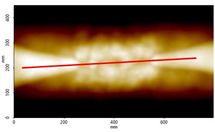 Figure 1. Contact mode AFM topography image of the vacuum-channel device's source-drain interface. The overlaid red line corresponds to the topography line profile displayed in Figure 2. Scan size: 450 x 800 nm.
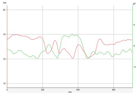 Figure 2. Line profiles of the AFM topography (red, left y-axis in nm) and the capacitance data (green, right y-axis in μV) of the device area scanned in Figures 1 and 3.
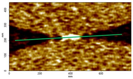
Figure 3. An SCM capacitance image of the region containing the device's source-drain in-terface. Brighter colors correspond to rela-tively more positively charged areas on the device whereas darker colors correspond to relatively more negatively charged areas. The overlaid green line corresponds to the capacitance line profile displayed in Figure 2. Scan size: 450 x 800 nm.
REFERENCES
1. Keys, A.S., Watson, M.D. (2007) Radiation Hardened Electronics for Extreme Environments, NASA Marshall Space Flight Center.
2. Vacuum Nanoelectronics: Interview with M. Meyyappan and Jin Woo Han. (2013) Retrieved from https://www.eeweb.com/blog/eeweb/interview-with-m.-meyyappan-and-jin-woo-han-on-vacuum-nanoelectronics
3. Scanning Capacitance Microsocpy (SCM). (2016) Retrieved from http://www.parkafm.com/index.php/park- spm-modes/94-electrical-properties/235-scanning-capacitance-microscopy-scm
4. Han, J.W., Meyyappan, M. (2014) Intro-ducing the Vacuum Transistor: A Device Made of Nothing, IEEE Spectrum. Re-trieved from http://spectrum.ieee.org/semiconductors/devices/introducing-the-vacuum-transistor-a-device-made-of-nothing
5. How AFM Works. (2016) Retrieved from http://www.parkafm.com/index.php/medias/nano-academy/how-afm-works