


Phani Kondapani, Gerald Pascual, Byong Kim, and Keibock Lee
Applications & Technical Marketing, Park Systems, Inc., Santa Clara, USA
Introduction
Semiconductor device dimensions have been moving to 1X-nm node and below for years now in order to continually meet market demand for faster and more efficient designs year-to-year. Device fabrication methods have improved all the way from 65 nm in 2006 to reaching the 1X node at 14 nm in 2014. Current projections by the International Technology Roadmap for Semiconductors have the first sub-1X node devices at 7 nm debuting as soon as perhaps 2017 [1]. To continue at this pace, manufacturers must have the capability to meet metrology requirements that simultaneously call for enhancements in resolution, precision, and accuracy. Tools to meet these needs must provide nanoscale imaging for critical dimension measurement and results that can be repeatable and accurate enough to enhance productivity in a mass production environment [2].
A compelling nanometrology solution for these challenges has been developed at Park Systems in the form of atomic force microscopy (AFM) tools with software specifically tailored for the automation of data acquisition and analysis. Named Park XEA [3], this software is designed to enable a process control engineer to use AFM systems to acquire accurate and repeatable nanoscale images of target devices according to user-defined procedures in custom recipe files. The corresponding increase in productivity makes this combined software and hardware solution attractive for wafer-level device fabrication plants everywhere.
Experiments
A three-inch patterned silicon wafer sample was used in this experiment. The target pattern on the wafer consists of rectangular pits which have pitches of 10 μm and step heights of 120 nm. Topography and roughness analysis at the target pattern was performed on two of pits. The sample was then mounted onto the stage of a Park NX-HDM AFM system [4] for imaging using the XEA software. AFM imaging in air was performed in non-contact mode using a silicon-based cantilever.
Five measurement locations were selected inside the wafer as shown in Figure 1a:
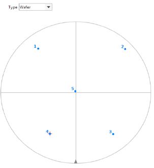 Fig. 1a – The five measurement sites selected for imaging from the sample patterned silicon wafer.
The reference measurement location (site #5 on Figure 1a) for creating the automated recipe was located at a NOR Gate device on the wafer. Four additional measurement sites of the same patterned device were selected at different XY coordinates inside the wafer to execute automated measurements of sample feature topography as well as roughness.
To begin creating the measurement and analysis recipe, the XEA software was put through a pair of teaching routines to allow it to optically recognize the location of the cantilever tip and sample pattern. These teaching routines (see Figures 1b and 1c) consist of optical image and XY stage adjustments and user-taught data fed into the software in order to guide the hardware to bring the target pattern measurement sites to the tip landing position.
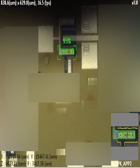
Fig. 1b – Optical camera feed from the XEA software interface displaying a 95% confidence level in the software’s ability to recognize the sample pattern.
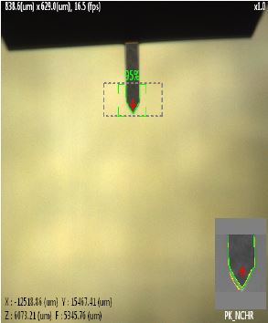
Fig. 1c – Optical camera feed from the XEA software interface displaying a 95% confidence level in the software's ability to recognize the cantilever. The red crosshair is a user-defined estimate of the cantilever tip's location.
Furthermore, the initial reference scan image of the sample pattern is used to adjust XY offsets in positioning when needed. For example, if a target pattern for study is not consistently optically recognizable by the software, a user can define the pattern’s location relative from a nearby landmark that is. Then the recipe would be designed to automatically move the sample to the cantilever tip accordingly using the landmark for orientation. This is done with nanometer-level precision in order to accurately image the user-defined region. With the teaching routines completed and XY offsets determined, scan parameters to acquire sample topography and roughness data are then defined by the user.
This entire set of calibrations and instructions is compiled into a recipe file that can now be used to run automated measurements on the sample. Immediately after each site is measured, the XEA recipe scripted to immediately conduct an automatic analysis of the collected data that completes. An aggregated report for the data acquired at each measurement site is then available after all measurement sites have been investigated and the recipe exhausted.
RESULTS & DISCUSSIONS
After the scanning was completed, we found the five user-defined measurement sites were accurately imaged with AFM. Their topography and roughness were measured simultaneously within the user defined locations as seen in green rectangles in the provided AFM images and the shaded blue columns in the line profiles included in Figures 2a – 2e. To determine the step height and roughness of the device within the user-defined area of interest, two locations were measured in each area: VZ1, located at the bottom of the first pit from the device's left edge, and Reference, a site on the raised area between the first pit and the second pit to its right.
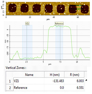 Fig. 2a – AFM topography image of measurement site #1 with green inset rectangle denoting specific area of interest. This area's line profile is also provided along with recorded step height (H) and roughness (R) values gathered by measuring sites VZ1 (in the sixth device pit) and Reference (in the raised area between the sixth and last device pits).
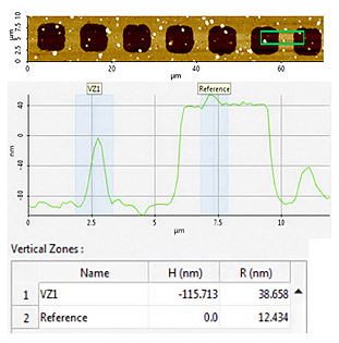 Fig. 2b – AFM topography image of measurement site #2, area of interest line profile, and collected step height (H) and roughness (R) values.
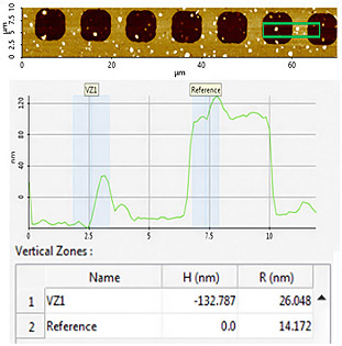 Fig. 2c – AFM topography image of measurement site #3, area of interest line profile, and collected step height (H) and roughness (R) values.
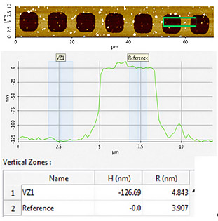 Fig. 2d – AFM topography image of measurement site #4, area of interest line profile, and collected step height (H) and roughness (R) values.
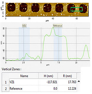 Fig. 2e – AFM topography image of measurement site #5, area of interest line profile, and collected step height (H) and roughness (R) values.
Step height was obtained by taking the difference between the average height calculated at a Reference location and the same calculated at the VZ1 location. This difference in height is also reflected in the color map used for the AFM images in Figures 2a – 2e as deeper, recessed features such as the pits have a darker color whereas the raised areas between them have a much lighter shade. Roughness values for the device were again calculated by scanning the specific locations VZ1 and Reference, with the pit floor roughness (at VZ1) being of more interest to us.
The collected data shows that the five sites have pits that are approximately 130 nm in height and pitches of 10 μm in length. Note the pitch length can also be repeatedly visually confirmed simply by looking at each AFM topography image in Figures 2a – 2e. Each topography image can also be used to visually confirm while the AFM did not scan the same exact area of interest at each measurement site, the degree to which each inset green rectangle was offset can be measured within a single micron—a remarkably small amount of variance given the automation employed in the study. The final step height and roughness values collected are made available in tabular form by the software after the user-defined recipe finishes running (see Table 1).
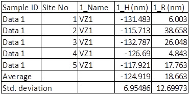 Table 1 – Step height (H) and roughness (R) values measured at each of the five selected sites with corresponding averages and standard deviations.
It is noted that the sample was exposed to ambient air for a significant amount of time prior to being scanned with the AFM. This caused sample contamination on several locations on the wafer including all measurement sites, but especially at sites 2 and 5. This correlates to the discrepancies depicted in the line profiles collected in Figures 2b and 2e and the roughness values shown at each of these two sites. The standard deviation in roughness is apparently larger than what would be expected for a pristine sample. This deviation may be attributable to the contaminants that collected on the sample's surface over an extended amount of time exposed to ambient air. This contamination had the unintended effect of further demonstrating the sensitivity of the AFM measurements and its ability to discern differences in features at nanoscale.
Summary
Five identical NOR Gate devices on a three-inch patterned silicon wafer consisting of rectangular pits with 10 um pitch and 120 nm step height were successfully imaged using a Park NX-HDM AFM system with XEA, an automation software from Park Systems. Through a user-defined recipe created by combining optical pattern recognition and the precision of AFM, accurate and repeatable nanoscale metrology with quantifiable data via automated data acquisition and analysis was demonstrated on all five patterns. Given this ability to automate data acquisition and analysis, this process has a viable application in similar fields. Fields such as bare silicon wafer manufacturing (surface roughness) and wafer design research (critical dimension measurement) are two areas of industry and research that routinely conduct studies that could dramatically increase their throughput and efficacy by incorporating a tool capable of fully automated AFM.
REFERENCES
[1] Moammer, K. (n.d.). TSMC Launching 10nm FinFET Process in 2016, 7nm in 2017 Read more: Http://wccftech.com/tsmcpromises- 10nm-production-2016-7nm- 2017/#ixzz4AXXp5M3v. Retrieved June 3, 2016, from http://wccftech.com/tsmcpromises- 10nm-production-2016-7nm-2017/
[2] J. Foucher; R Therese; Y. Lee; S.-I. Park; S-J. Proc. SPIE 8681, Metrology, Inspection, and Process Control for Microlithography XXVII, 868106 (April 18, 2013); doi:10.1117/12.2011463
[3] Park NX-HDM features - Automatic Measurement Control. (n.d.). Retrieved June 03, 2016, from http://www.parkafm.com/index.php/product s/industrial-afm/park-hdm/applications
[4] Park HDM - Overview | Park Atomic Force Microscope. (n.d.). Retrieved June 3, 2016, from http://www.parkafm.com/index.php/product s/industrial-afm/park-hdm/overview