
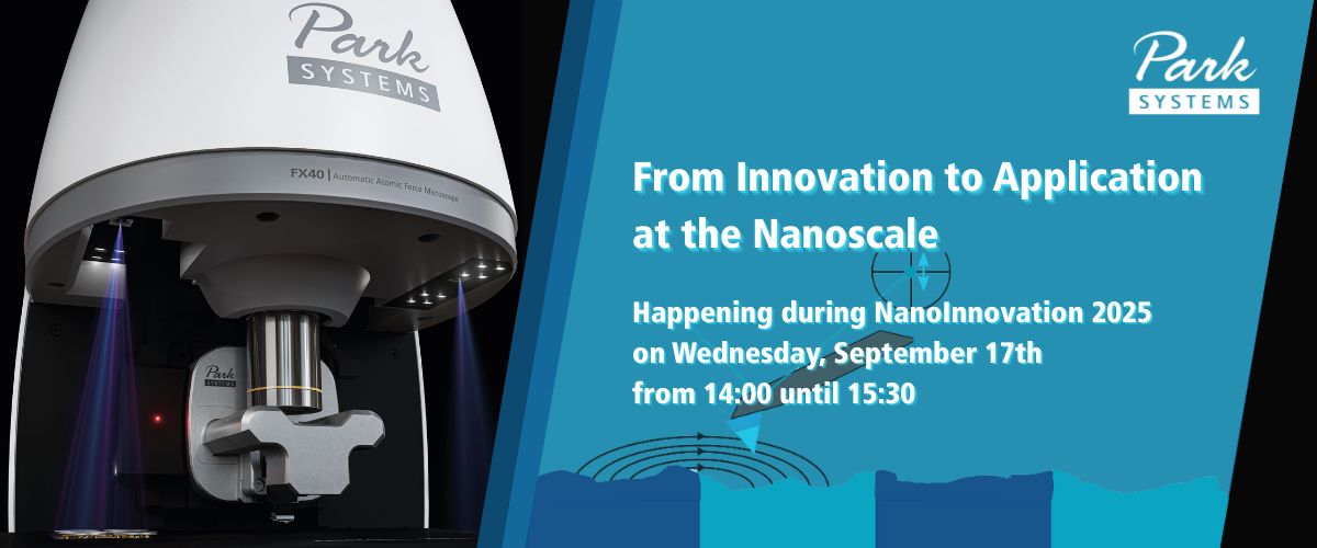
Join us and our Italian Distributor Gambetti Kenologia Srl in Rome this September at the NanoInnovation 2025 where we will exhibiting as well as hosting a workshop and live demo.
Workshop: From Innovation to Application at the Nanoscale
Date: Wednesday, 17 September 2025
Time: 14:00 – 15:30
Discover how Atomic Force Microscopy (AFM) is transforming nanotechnology research and applications. This 90-minute workshop features three expert talks:
- Dr. Elena Arbelo Jorge – Introduction to Park Systems’ newest AFM solutions
- Dr. Jonathan Moffat – Advanced materials characterization with AFM
- Dr. Christian Martella – Multifunctional AFM approaches for 2D materials and device integration
______________________________
Abstract Dr. Elena Arbelo Jorge
Market Development Manager Europe, Park Systems Europe, Mannheim, Germany
Email: elena.arbelo@parksystems.com
An introduction to the newest Park Systems' nanoscale microscopy solutions. Empowering innovation across nanotechnology applications
Atomic Force Microscopy (AFM) stands as a versatile and high-resolution tool for the characterization of advanced nanomaterials, offering powerful capabilities that extend far beyond topographical imaging. Its strength lies in the ability to perform correlative measurements of multiple physical properties—such as electrical conductivity, surface potential, nanomechanical stiffness, and even local chemical composition—all at the nanoscale.
In this presentation, we introduce the new FX Atomic Force Microscopy (AFM) series, which boasts a high level of built-in automation features that set it apart from other research AFMs on the market. Automation reduces the amount of manual handling of the equipment, thereby facilitating its use. It also dramatically reduces set-up time and eliminates user error and equipment breakage. An overview on the different key features and advantages of these series and different models will be presented.
We demonstrate this series to be the easiest, most versatile and cutting-edge platform for investigating a range of features on a nanometer scale such as 2D materials, low-dimensional optoelectronics, biopolymers, nanoparticles and nanofabricated devices.
During this symposium we prove Park Systems AFMs to be an indispensable, multi-functional platform for comprehensive nanoscale characterization across disciplines.
______________________________
Abstract Dr. Jonathan Moffat
Applications Scientist, Park Systems UK, Nottingham, UK
Email: Jonathan.moffat@parksystem.com
Advanced materials characterisation with atomic force microscopy
Atomic force microscopy (AFM) is a highly versatile tool for providing characterisation of materials and devices at the nanoscale. AFM is well known to provide topographical information such as roughness and morphology, but there are a number of different measurement modes that go beyond topography and provide a deeper understanding of materials and device properties. This talk will give a brief introduction to the wide variety of measurement modes available with AFM, including electrical modes such as Kelvin probe force microscopy (KPFM), piezoresponce force microscopy (PFM) as well as nanomechanical characterisation. Examples of how these measurement modes can be applied will also be discussed. These include:
- Investigation of 2D materials, where combined correlative imaging, by seamlessly switching between techniques like conductive AFM (C-AFM) and Kelvin probe force microscopy (KPFM), allow for fast same area mapping of local electronic heterogeneities and defects down to the atomic level.
- Measurements of low-dimensional optoelectronic materials, which enables simultaneous assessment of morphology, charge transport, and photonic response, crucial for understanding structure-property relationships.
- Characterization of nanoparticles where AFM has the ability to resolve size, shape, aggregation state, and local electronic behavior at the single-particle level.
- Nanofabricated device measurements, where high throughput with sub-nanometer precision is achieved in measuring critical dimensions and defects, while also evaluating local electrical and mechanical performance.
______________________________
Abstract Dr. Christian Martella
National Research Council, Institute for Microelectronics and Microsystems (CNR IMM), Unit of Agrate Brianza, via C. Olivetti 2, Agrate Brianza 20864, Italy,
E-mail: christian.martella@cnr.it
Multifunctional approaches for exploring 2D materials and their device integration via Atomic Force Microscopy
Atomic force microscopy (AFM) represents a powerful toolbox for exploring the physics of two-dimensional (2D) materials and accelerating their integration into next-generation optoelectronic devices. In this talk, we demonstrate how advanced AFM (including Kelvin probe force microscopy KPFM, electrostatic force microscopy EFM, and conductive AFM C-AFM) provide key insights into the structure–function relationships in MoS₂ and Te nanosheets grown via chemical or vapor-phase techniques. Three case studies are presented. First, KPFM reveals how substrate induced ripple morphologies in CVD-grown MoS₂ generate directional anisotropy and localized charge doping, which are crucial for anisotropic optoelectronic responses. [1] Secondly, EFM measurements show that the choice of molecular seeding promoters drastically modulates the electronic polarizability of monolayer MoS₂, significantly impacting photoluminescence and critically altering charge transport in back-gated field-effect transistors. [2] Finally, C-AFM enables direct nanoscale mapping of resistive switching behavior in vapor deposited 2D tellurium, demonstrating its integration in memristor devices for neuromorphic computing. [3] The use of gold substrates enhances the switching efficiency by facilitating interfacial reconfiguration and reducing energy consumption. In perspective, these studies illustrate how AFM techniques are not only indispensable for fundamental characterization, but also for correlating local physical properties with device performance, paving the way for the rational design of 2D material-based transistors and memory elements.
[1] C. Martella, C. Mennucci, E. Cinquanta, A. Lamperti, E. Cappelluti, F. Buatier de Mongeot, A. Molle, Anisotropic MoS2 Nanosheets Grown on Self-Organized Nanopatterned Substrates Adv. Mater. 2017, 29, 1605785.
[2] C. Martella, E. Kozma, P. P. Tummala, S. Ricci, K. A. Patel, A. Andicsovà-Eckstein, F. Bertini, G. Scavia, R. Sordan, L. G. Nobili, M. Bollani, U. Giovanella, A. Lamperti, A. Molle, Changing the Electronic Polarizability of Monolayer MoS2 by Perylene-Based Seeding Promoters. Adv. Mater. Interfaces 2020, 7, 2000791. https://doi.org/10.1002/admi.202000791
[3] S. Ghomi, C. Martella, Y. Lee, P. H.-P. Chang, P. Targa, A. Serafini, D. Codegoni, C. Massetti, S. Gharedaghi, A. Lamperti, C. Grazianetti, D. Akinwande, A. Molle, Non-Volatile Resistive Switching in Nanoscaled Elemental Tellurium by Vapor Transport Deposition on Gold. Adv. Sci. 2025, 12, 2406703. https://doi.org/10.1002/advs.202406703
______________________________
Live Demo: Precision in Practice – The FX40 AFM
Date: Thursday, 18 September 2025
Time: TBC
This demonstration will show live atomic force microscopy (AFM) measurements on the FX40 microscope from Park Systems. The FX40 is a fully equipped AFM that combines high performance with superior ease-of-use. Tip exchange and alignment is fully automated, meaning handling of probes with tweezers is a thing of the past. A sample view camera allows the user to pick and choose locations to carry out a series of automated measurements. The demonstration will show all these features and more, including the acquisition of measurements in real time. The demonstration will also show how we can seamlessly switch between measurement modes without hardware changes, where we can carry out Kelvin probe force microscopy (SKPM) and conductive-AFM (C-AFM) at the same location by simply switch settings in the software.
Dr. Jonathan Moffat will demonstrate key modes including:
- Basic HW overview: controller, main body, head
- Software overview
- Automated tip exchange
- Sample navigation and StepScan
- Run a basic topography image with a well defined topography
- Switch to KPFM which would then show changing probe and samples.
See how automation and versatility come together in one powerful platform.
______________________________
Link: https://www.nanoinnovation2025.eu/home/
Please contact Michela Rizzi to save yourself a slot at the workshop and demo.